 Local solid phase growth of few-layer graphene on silicon carbide from nickel silicide supersaturated with carbon
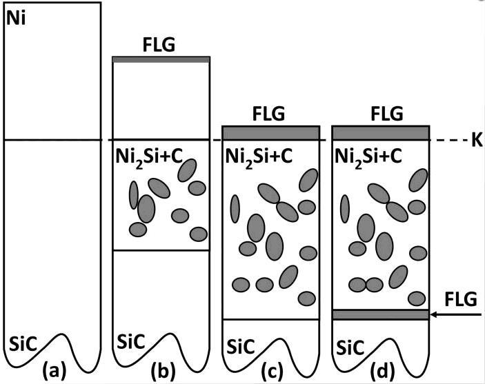
Patterned few-layer graphene (FLG) films were obtained by local solid phase growth from nickel silicide supersaturated with carbon, following a fabrication scheme, which allows the formation of self-aligned ohmic contacts on FLG and is compatible with conventional SiC device processing methods. The process was realised by the deposition and patterning of thin Ni films on semi-insulating 6H-SiC wafers followed by annealing and the selective removal of the resulting nickel silicide by wet chemistry. Raman spectroscopy and X-ray photoelectron spectroscopy (XPS) were used to confirm both the formation and subsequent removal of nickel silicide. The impact of process parameters such as the thickness of the initial Ni layer, annealing temperature, and cooling rates on the FLG films was assessed by Raman spectroscopy, XPS, and atomic force microscopy. The thickness of the final FLG film estimated from the Raman spectra varied from 1 to 4 monolayers for initial Ni layers between 3 and 20 nm thick. Self-aligned contacts were formed on these patterned films by contact photolithography and wet etching of nickel silicide, which enabled the fabrication of test structures to measure the carrier concentration and mobility in the FLG films. A simple model of diffusion-driven solid phase chemical reaction was used to explain formation of the FLG film at the interface between nickel silicide and silicon carbide.
Go back