 Charge Transfer and Quantum Emitters in Two-Dimensional Heterostructures: An Ab Initio Study
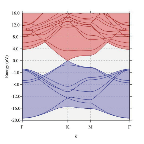
An essential requirement for the physical implementation of quantum communication and a range of other quantum technologies is the realisation of bright and deterministic sources of single photons. Such quantum emitters have been recently discovered in 2D hexagonal boron nitride (h-BN) and are the result of defect states located deep in the large bandgap of h-BN. Furthermore, there has been increasing interest in using these defects for optically addressable spin qubits in h-BN. Control over the charged states of these defects is essential to achieve stable operation of quantum emitters and/or spin qubits based on such defects. Recent experimental studies have shown that quantum emitters in h-BN can be spectrally quenched when deposited on functionalised graphene and spatially quenched when deposited on patterned graphene, suggesting the existence of charge transfer processes occurring between the h-BN and graphene layers. However, a rigorous theoretical study on the types of h-BN defect states involved in charge transfer and the modification of defect properties in such a heterostructure (e.g. defect energy levels and formation energies) is still lacking. Here, we present the results of an investigation of charge transfer levels of quantum emitters in an h-BN/graphene heterostructure using density functional theory. Specifically, we perform simulations of native h-BN defects — nitrogen vacancies (VN), boron vacancies (VB), nitrogen antisite (NB), and boron antisite (BN) — and explore the possibility of charge transfer in such a 2D heterostructure.
Go back