Direct measurement of residual stress in integrated circuit interconnect features
A.B. Horsfall1, J.M.M. dos Santos1, S.M. Soare2, N.G. Wright1, A.G. O’Neill1, S.J. Bull2,
A.J. Walton3, A.M. Gundlach3, J.T.M. Stevenson3
1 School of Electrical, Electronic and Computer Engineering, University of Newcastle, Newcastle, NE1 7RU, UK
2 School of Chemical Engineering and Advanced Materials, University of Newcastle, Newcastle, NE1 7RU, UK
3 Scottish Microelectronics Centre, University of Edinburgh, EH9 3JL, UK
Abstract:
The process induced stress in interconnect features has a direct influence on the lifetime of the integrated circuit. We have demonstrated the first direct measurement of stress in a single interconnect feature by means of a novel stress sensor, fabricated in a CMOS compatible process. The sensor we have developed is shown to have the ability to display the residual stress in the feature as a rotation. Due to the inherent scalability of the structure it is suitable for use in a production environment for state-of-the-art chips.
1. Introduction
The continuing drive towards deep sub-micron silicon technology has been stimulated by the demand for higher operating frequencies, greater circuit complexity and lower power consumption. As gate lengths approach 50 nm and below for commercial processes there is a demand for interconnect track widths to decrease and the number of levels of interconnect to increase. This trend leads to higher current densities in the interconnect tracks as well as placing unprecedented demands on scientists and engineers to deliver metallisation of ever higher quality. The severe geometric constraints laid on such narrow lines reduces their ability to relax stress by plastic deformation. These stresses in turn increase the diffusion of metal ions leading to premature track failure. Moreover, the shrinking lateral dimensions of all integrated circuit components mean that less ion diffusion is necessary before line failure occurs.
Without doubt, the major cause of failure and yield problems is the back-end-of-line metallisation. A feature which has received little attention until recently is the impact of mechanical stress on the reliability of the interconnect. Although there is phenomenological evidence for the formation of voids at triple points, in narrower metal tracks voids form more frequently at the surface (albeit at a grain boundary junction) and tracks can fail even before the onset of any electromigration. In these cases stressmigration is believed to be responsible. Here void nucleation and growth has been suggested to be the result of the metal track trying to relax in a confined environment. The metal stress is largely caused by the thermal expansion mismatch, during the manufacturing process, between the track and the silicon substrate, with further constraint imposed by the intermetal dielectric. The processing can cause a tensile stress in the track larger than the yield stress in the metal. The metal tries to shrink but is prevented by its adhesion to the intermetal dielectric. Thus it must relieve the stress by void formation and growth.
A rapid introduction of new materials and processes is necessary in the coming years to meet resistivity and low/high k targets and address system on chip needs, which will generate chip reliability exposure, according to the ITRS. There are relatively few measurements of the stresses generated in metallisation structures and how these are changed by processing. There is growing evidence that the key to understanding the reliability issues associated with metallisation is to understand the initial conditions of the lines immediately following processing. Stress induced metal extrusions and void formation during annealing have been observed in both Cu metallisation schemes, by Iguchi et al [[i]], and Al, by Shibata et al [[ii]].
The measurement of stress in sub-micron tracks presents a major challenge. The techniques most widely used involve x-ray diffraction [[iii]], where the stress of a thin film can be evaluated but the lateral dimensions of the film must be greater than the spot size of the beam, which is limited to 1mm. Another technique to quantify stress is by measuring wafer bowing, which cannot be applied to a single metal stripe, but would have to be averaged over a wafer patterned with many similar stripes. Routine in-line monitoring of stress is not realistic using these techniques. There is therefore a need for new methods of measuring stress in metal interconnects. One solution to this problem is to develop a test structure which can be fabricated on the wafer along with devices and used to monitor stress generation and relaxation as a function of processing. A rotating beam sensor design, as shown in figure 1 has potential for fulfilling this function for both Al and Cu technologies. Such a sensor will continue to work as critical dimensions reduce and does not require expensive specialist measuring apparatus.
In this paper we report the first results of a rotating beam stress sensor for integrated circuit metallisation. A design study using the finite element package ANSYS is described in section 2, while the fabrication process described in section 3 was used to demonstrate a range of stress sensors as shown in section 4.
2. Sensor Design
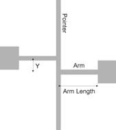
The rotational sensor is shown diagramatically in figure
1. As can be observed from the figure, when the fixed beams (labelled as arms) are freed from the underlying dielectric layer, they contract or extend in order to relieve the residual tensile or compressive stress. These two arms are connected off centre on opposing sides of the rotating beam (pointer) as shown in the figure. Any deviation in the length of the arms exerts a torque about the centre of the sensor structure, causing a rotation of the pointer arm.
A commercial finite element software package (ANSYS) has been used to model the rotation of the structure in terms of the process conditions and materials properties of the aluminium layer. The plasticity and creep properties of thin films are not the same as those observed for bulk materials and input parameters for the modelling have been determined by nanoindentation testing in conjunction with finite element modelling [[iv]].
Figure 1 – Schematic diagram of the sensor structure
Initial simulation of the sensor rotation using aluminium elastic/plastic behaviour represented by a bilinear hardening model showed that creep has little or no effect on performance. The variation of deflection with physical dimensions is similar to that observed previously for polysilicon and silicon nitride [[v]], however the plastic deformation of the soft aluminium has a much more significant effect, reducing rotation compared to the harder materials. To reduce the effects of plasticity and increase sensitivity, key sensor dimensions must be reduced greatly. The most critical dimension is the arm separation, which in the elastic – plastic regime gives rise to the deflection shown as the simulated curve in figure 4. This would suggest that a sensor with an arm separation close to the width of the pointer feature will give the highest rotation, although the deformation of the intersection of the arms and pointers (hinge), as can be seen in figure 2, implies that this requires a very controlled lithography and etch process step.
The equation of best fit to these simulated data points is given by
![]() (1)
(1)
the form of which agrees with calculations based on the difference in thermal coefficient of expansion of the aluminium layer and silicon substrate [[vi]].
3. Fabrication
The sensors were fabricated on three inch n-type silicon wafers of thickness 380mm. After cleaning, 0.1mm of TiN was sputter deposited to act as an etch stop layer, before 2um of PECVD SiO2. 1mm of aluminium was then sputtered using a Balzers BAS 450, operating at 2kW target power and 600V target bias in an argon atmosphere of pressure 2´10-3 mBar. After lithography using Shipley SPR2 photoresist and a 5´ wafer stepper, the aluminium was patterned using a chlorine plasma in a STS reactive ion etcher. The wafers were then subject to a sinter process in forming gas to densify the metallization and reduce any aluminium oxide formed during the sputtering. This process ramped the wafers to 435oC, held them there for 25 minutes with 40/60 H2/N2 forming gas flowing and allowed them to cool in air. After sintering, the wafers were then diced into chips to aid ease of handling. The final process step is the isotropic reactive ion etch step which is required to release the structures from the silicon dioxide underneath. After processing, the rotation of the devices is measured using a CamScan scanning electron microscope with digitising frame grabber.
4. Results and Discussion
Figure 2 shows electron micrographs of the released sensors for devices fabricated with a 2mm feature width and 140mm arm length. The anticlockwise rotation of the pointer arm clearly shows evidence of tensile stress in the layer, which is as a result of the sintering process. The dark areas in the pictures show the detachment of the TiN etch stop layer, revealing the silicon surface beneath, suggesting a small amount of over etch during the isotropic release etch at the end of processing.
Figure 3 shows the angle of rotation of the sensor structure as a function of arm separation for two different arm lengths, 110 and 140mm. The trend lines on the fits have been calculated by using regression analysis based on equation 1, which was extracted from the ANSYS simulation results. This yields fit equations of
![]() (2)
(2)
for the 140mm arm devices and
![]() (3)
(3)
for the 110mm arm devices.
Sensor structures fabricated with an arm separation of 2mm, as shown in figure 4, have a lower angle of rotation than those fabricated with an arm separation of 4mm. This is due to the excessive plastic deformation of the arm/pointer intersection (hinge) with the release in stress. Because of this excessive deformation in this central region of the pointer, structures with this arm separation are considered to be more likely to fail mechanically and show lower sensitivity to stress. For this reason, these structures are not considered further in this work.
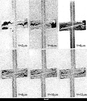
Figure 2 – Electron Micrographs of released sensors with arm lengths of 140mm, showing the effect of arm separation. The scale bar represents 30mm.
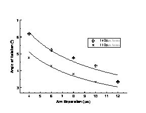
Figure 3 – Variation of angle of rotation as a function of arm separation for fabricated sensors and the simulated data for an arm length of 140mm.
The discrepancy between the fit equations for the simulated an experimental data arises from two main sources. The exponential term (0.822 for simulated and 0.47 for experimental) is dependent on the definition of the intersection between the arms and pointer. The simulated structure comprises perfectly sharp features at this intersection. Including a more realistic shape at these hinge points, by the use of a fillet defined by a radius of curvature, reduces the value of the exponent in the equation as summarised in table 1.
|
Radius of Curvature (mm) |
Exponent |
|
0 |
0.82 |
|
2 |
0.73 |
|
5 |
0.71 |
|
10 |
0.67 |
Table 1 – Variation of curve fitting parameters with radius of curvature of the hinge structures
This data suggests that in order to achieve the exponent observed with the experimental data of 0.47, would require a radius of curvature of 27.1mm. The hinge shape in the fabricated structures, has a radius of curvature closer to 2mm. Hence, although the modification of the hinge structure in this way does not give results equal to those observed experimentally, it can be seen that a more realistic behaviour can be simulated.
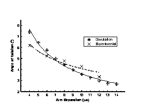
Figure 4 – Variation of the rotation angle with material parameters and hinge detail for a fabricated sensor structure
The absolute value of the rotation observed is affected by the material parameters used for the simulation. The curves in figure 7 show the effects of changing the value of yield stress in the simulation. The lowest line is using the yield stress of 160MPa, the vale observed in bulk aluminium samples, whilst the upper most line represents a yield stress of 500MPa, the value extracted from nanoindenation of thermally evaporated aluminium on silicon substrates. From this, it can be seen that a yield stress of approximately 440MPa, the middle line, gives the value of rotation closest to the experimental values for an arm separation of 4mm.
5 Conclusions
We have shown that the stress in sub-micron interconnect features, a major factor in the reliability of integrated circuits, can be measured using a rotating sensor structure. This rotation, which is observable with a reflected light microscope, is suitable for use in a process environment. We have shown that the comparison of the rotation predicted by finite element simulation and that observed in experimental structures is critically dependent on the pattern transfer of the lithographic process and the yield stress value used in the simulation. The optimum device is shown to be one in which the arm separation is double the pointer width, as this offers the highest value of rotation and avoids excessive deformation of the structure in the hinge area.
[i] M. Iguchi, et al, IEDM Tech Dig, (1999), p615
[ii] H. Shibata, et al, Jpn. J. App. Phys., 33, p1814, (1994)
[iii] P. Besser, AIP Conf. Proc. 491, p229, (1999)
[iv] S.M. Soare et al, submitted to Surface and Coatings Technology
[v] X. Zhang, et al, Thin Solid Films, 335, p97, (1998)
[vi] S.H. Lee, et al, Thin Solid Films, 341, p136, (1999)