J. Cortadella - M. Kishinevsky - A. Kondratyev - L. Lavagno - A. Yakovlev
ASYNC'2000, Eilat, Israel
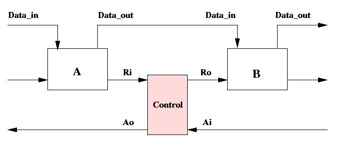
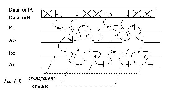
Figure 1 shows a data processing structure consisting of two computation blocks, A and B, and a control circuit. The goal is to design the speed-independent control circuit. Different control disciplines are possible. Let us assume that we have chosen a discipline, called half-handshake. It is shown in Figure 2. This discipline assumes that the datapath includes latches which are transparent to input data when the control signal is low and which are opaque, i.e. insensitive to its data input, when the control is high. E.g. the latch in B is transparent when Ro=0 and opaque when Ro=1. Furthermore we assume that the fact that Ri becomes 1 indicates that the data in the previous stage, stage A, is captured and stable (after that stage has become opaque).
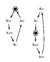
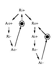
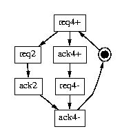
The STG specifying the half-handshake control circuit is given in Figure 3. Signals Ri and Ai are inputs, and Ao and Ro are outputs. Output Ro can be seen as a latch enable signal for the data path. Output Ao is an acknowledgement signal sent to the previous control stage.
Figure 1: A data processing structure.
Figure 2: Half-handshake discipline: timing diagram.
Figure 3: An STG for the half-handshake:
(a) independent handshakes at the left and right ports
(b) unbounded version with , (c) version with
CSC-violation, (d) final version with CSC and a redundant arc removed
draw_astg half-hand.g | ghostview -
draw_astg -nofold  half-hand.g | ghostview -
draw_astg -noinfo  -bw half-hand.g | ghostview -
draw_astg half-hand.g -o half-hand.g.ps
ghostview half-hand.g.ps
The -nofold option draws vertically as much as possible, while the -noinfo option removes the signal legend.
write_sg half-hand.g | draw_astg -sg | ghostview -
write_sg half-hand.g -o  half-hand.sg
draw_astg -nofold  half-hand.sg | ghostview -
write_sg -bin half-hand.g  -o  half-hand.bin.sg
draw_astg -sg half-hand.bin.sg | ghostview -
draw_astg -bin half-hand.bin.sg | ghostview -
draw_astg -sg -noinfo -nonames -bw half-hand.bin.sg | ghostview -
The -bin option of write_sg generates a binary encoding for all states and checks for CSC violations, if any (i.e., pairs of states with the same code and different enabled output signals). The -bin option of draw_astg understands this notation and highlights violations.
write_sg half-hand.g -o half-hand.sg
write_sg -bin half-hand.g | draw_astg -bin | ghostview -
write_sg -bin half-hand.g | draw_astg -bin | ghostview -
petrify  half-hand.g -cg -eqn  half-hand.cg.eqn -o  half-hand.out
more  half-hand.cg.eqn
draw_astg half-hand.out | ghostview -
Note also how petrify removed the redundant arc in the half-hand.out output STG.
The implementation that petrify obtained for the STG with increased concurrency and the CSC problem in this case has exactly the same complexity (but a slightly different form) as the one obtained for the case without the CSC problem. This does not happen in general, and concurrency reduction is often a good way to trade off logic complexity and performance.
petrify  half-hand.g -gc -eqn  half-hand.gc.eqn -no
more  half-hand.cg.eqn
more petrify.log
The petrify.log file also reports technology-independent performance information, such as:
In the part of the file labeled Input -> Input Delays the numbers in parentheses denote the number of output events between the corresponding pair of input events. You should look at the output STG to understand the numbers, and consider that the path Ri+ -> Ro+ -> Ao+ -> Ro- -> Ai+ is not a worst-case path under the hypothesis of slow input events, because Ai+ will always determine the firing time of Ro+.
petrify  half-hand.g -lit3 -tm -eqn  half-hand.lit3.eqn -no
petrify  half-hand.g -lit2 -tm -eqn  half-hand.lit2.eqn -no
more  half-hand.lit3.eqn
more  half-hand.lit2.eqn
Note that if we only use -tm (technology mapping), petrify generally decomposes logic until some gate is found that matches each signal (modulo inverters). If -lit3 -tm is used, then we force decomposition into 3-literal functions, and then technology mapping is applied. In general, it is not clear what the best option out of -litN is. Sometimes, doing a more aggressive decomposition allows a better sharing of gates. Another reason for improvement is that finer decomposition allows a better exploration for matching gates by trying to collapse with different neighbours. A reason for worse results is that more decomposition may require extra acknowledgement wires.
petrify  half-hand.g -latch C -tm -eqn  half-hand.cel.eqn -no
more  half-hand.cel.eqn
petrify  half-hand.g -latch SRD -tm -eqn  half-hand.srd.eqn -no
more  half-hand.srd.eqn
Note that in the actual implementation we can use the inverted version of [1] (hence have a three-input NOR instead of OR) and apply it directly to the input of the Set-dominant latch for [Ro]. Note also that the output of the inverter gate [0] is not acknowledged (when switching from 0 to 1), and hence its delay must be smaller than that of the rest of the logic (labelled as PRAGMA in file half-hand.srd.eqn). In particular, if it is slow in going from 0 to 1, signal [1] (in its inverted implementation) might have a hazard as a result of Ao-after Ai- when it is still [0]=0. This hazard may propagate to the primary output [Ro].
petrify  half-hand.g -nolatch -tm -eqn  half-hand.nolatch.eqn -o half-hand.out
more  half-hand.nolatch.eqn
draw_astg half-hand.out | ghostview -
To summarise our use of latches, here is the comment from the petrify manual page. The -latch str option specifies a restricted set of latches to be used for synthesis; str can contain any string of characters from the set CDRS, which respectively correspond to the following latches: Muller C element, D latch, reset-dominant SR latch and set- dominant SR latch. These latches are only used if found in the library. In case this option is not specified, any asynchronous latch in the library is used.
petrify  half-hand.g -topt -cg -eqn half-hand.topt.cg.eqn -no
more half-hand.topt.cg.eqn
more petrify.log
Explain why adding other timing assumptions between inputs and outputs, such as .time Ao-<|Ai- and .time Ro-<|Ri-, may be wrong if we have no more information about relative timing between the left and right hand side parts of the environment.
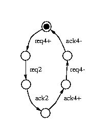
Figure 4 depicts the interface of 2-to-4 and 4-to-2 phase converters.
Figure 4: 2-to-4 and 4-to-2 phase converters
A 2-to-4 phase converter can be described by the following regular expression:
Here events req2 and ack2 stand for either rising or falling transitions on the 2-phase handshake.
A 4-to-2 phase converter can be described similarly by the following regular expression (as well as by other, more concurrent, specifications described in the 4-to-2 exercise):
write_sg -bin conv24.g | draw_astg -bin | ghostview -
petrify -untog conv24.g -o conv24.untog.g
draw_astg conv24.untog.g | ghostview -
petrify  conv24.g -cg -eqn  conv24.cg.eqn -o  conv24.out
more  conv24.cg.eqn
draw_astg conv24.out | ghostview -
petrify conv24.g -latch SRD -tm -eqn conv24.srd.eqn -no
more  conv24.srd.eqn
Note that in this example, petrify is overly conservative about zero-delay inverters (cf. PRAGMA in front of [2]). The output of [2] is actually acknowledged: we have to re-draw the circuit in conv24.srd.eqn in such a way that [2] is connected to both the OAI12 gate for [req4] but also to the NAND2 gate for [1] (instead of req2 being lised there. Indeed, [1] = [2]' + csc0' would have been a much `cleaner' NAND2. With a bit more thought, one can recognise that the combination of NAND2 [1] and OAI12 [req4] implements an XOR2 function.
petrify conv24.g -mc -eqn conv24.mc.eqn  -no
more conv24.mc.eqn
Compare this solution with the previous one.
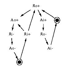
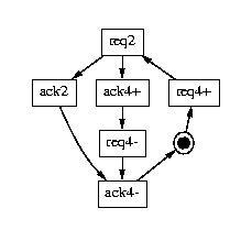
Figure 5 shows three different specifications for a 4-to-2 phase converter, with different degrees of concurrency between inputs and outputs. The third version has the highest potential performance, because it has only one output transition between any two input transitions, and it performs the 4-phase reset (ack4+ and req4-) completely in parallel with the 2-phase handshake. Of course, its logic cost is also greater.
Figure 5: Specifications of 4-to-2 phase converters.
petrify -untog conv42_seq.g -o conv42_seq.untog.g
draw_astg conv42_seq.untog.g | ghostview -
petrify conv42_par.untog.g -cg -eqn conv42_par.eqn  -o  conv42_par.out
more conv42_par.eqn
draw_astg conv42_par.out | ghostview -
Note how the number of CSC conflicts, and hence the number of state signals and the logic complexity, grows with the increase in concurrency. As usual, performance increase roughly implies area increase.
.time req2-=ack4+/1@ack2-,req4-/1
.time req2+=ack4+@ack2+,req4-
The first constraint means that for both ack2- and req4-/1 the firing times of req2- and that of ack4+ are undistinguishable. Hence ack2- could be enabled by req4-/1 just as well (instead of req2- as in the original specification) without changing the observable firing sequences.
For that, use:
petrify conv42_par.untog.g -topt -cg -eqn conv42_par.t.eqn -o conv42_par.t.o
more conv42_par.t.eqn
draw_astg conv42_par.t.o | ghostview -
Compare the solutions with the untimed implementation.
Examine the contents of the petrify.log report file.
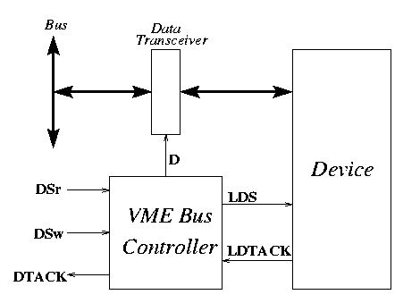
Figure 6 depicts the interface of a slave device to a VME bus. What is shown here is the result of an abstraction of the main synchronization core between the bus and the device links, separately from all remaining logic. The latter performs address and opcode decoding, error detection and some other functions that are outside this controller.
The behavior of the controller is as follows: a request to read from or write into the device is received by one of the signals DSr or DSw respectively. In a read cycle, a request to read is sent to the device through signal LDS. When the device has the data ready (LDTACK), the controller must open the transceiver to transfer data to the bus (signal D, which is a Data Enable signal; it controls the transceiver together with a direction signal provided in the bus, namely it closes one latch and opens the tri-state in one direction, and opens the other latch in the other). In the write cycle, data is first transferred to the device by opening the transceiver (D). Next, a request to write is sent to the device (LDS). Once the device acknowledges the reception of the data (LDTACK) the transceiver must be closed to isolate the device from the bus. Each transaction must be completed by a return-to-zero of all interface signals, seeking for a maximum parallelism between the bus and the device operations.
Figure 6: VME bus controller
 (a)
(a)
 (b)
(b)
 (c)
(c)
 (d)
(d)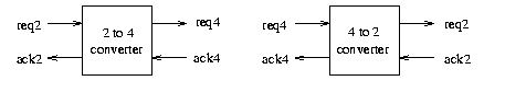
 (a)
(a)
 (b)
(b)
 (c)
(c)